Gemini Stimdeck
geminicomplex.comAn FPGA-based miniaturized ATE for integrated circuits, taken from conception to working product. It drives and samples logic on a 400-channel test bus to functionally test any attached device. A 12-layer triple-FPGA motherboard, a custom vector processing unit with its own ISA, a Linux board support package, and a compiler for the test pattern language. Hardware, RTL and software, solo.
Specs
| Test bus I/O | 400 digital channels |
| Vector execution speed | 50 Mbps per channel |
| Per-channel vector burst depth | 67M vectors |
| Latency | sub-10 ns |
Why
The vector engine runs on FPGA fabric with its own DDR3. No CPU is in the path from pattern to pins, so the interval between one vector and the next is set by the fabric clock rather than by software.
400 channels at 50 Mbps each, a 50 MHz vector rate, sub-10 nanosecond latency, and 67M vectors of burst depth per channel. Patterns are written in Dots, compiled, and queued from a web app that reports pass or fail per pin.
Architecture
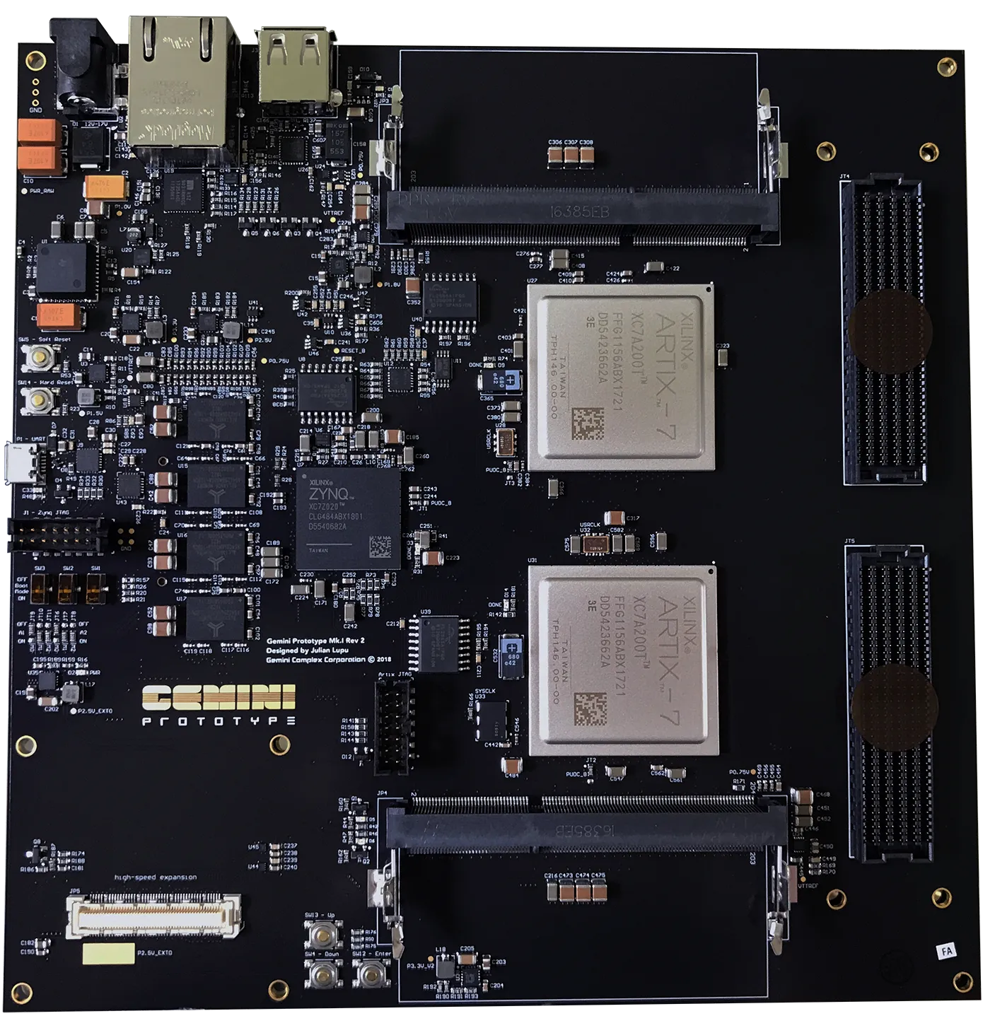
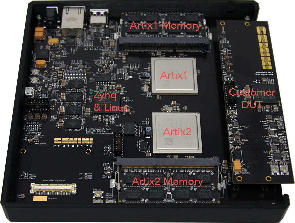
Three FPGAs. A Zynq-7000 SoC called Agent orchestrates the boot process, services the test queue and serves the web app. Two Artix-7s, Castor and Pollux, each run a vector processing unit against their own 8GB of DDR3 tester memory. The board runs VecOS, an operating system built to do nothing but execute test patterns.
VecOS is a board support package I built up from parts: a custom Linux kernel and device tree, a root filesystem and init scripts, a U-Boot second-stage bootloader, and a set of cross-compiled binaries. There is no BIOS underneath it.
Work arrives over NFS as compiled stim binaries and prgm files, queued from the web app. Agent runs queued programs as slots open, then records pass or fail for every execution in an on-board SQLite database.
The vector processing unit
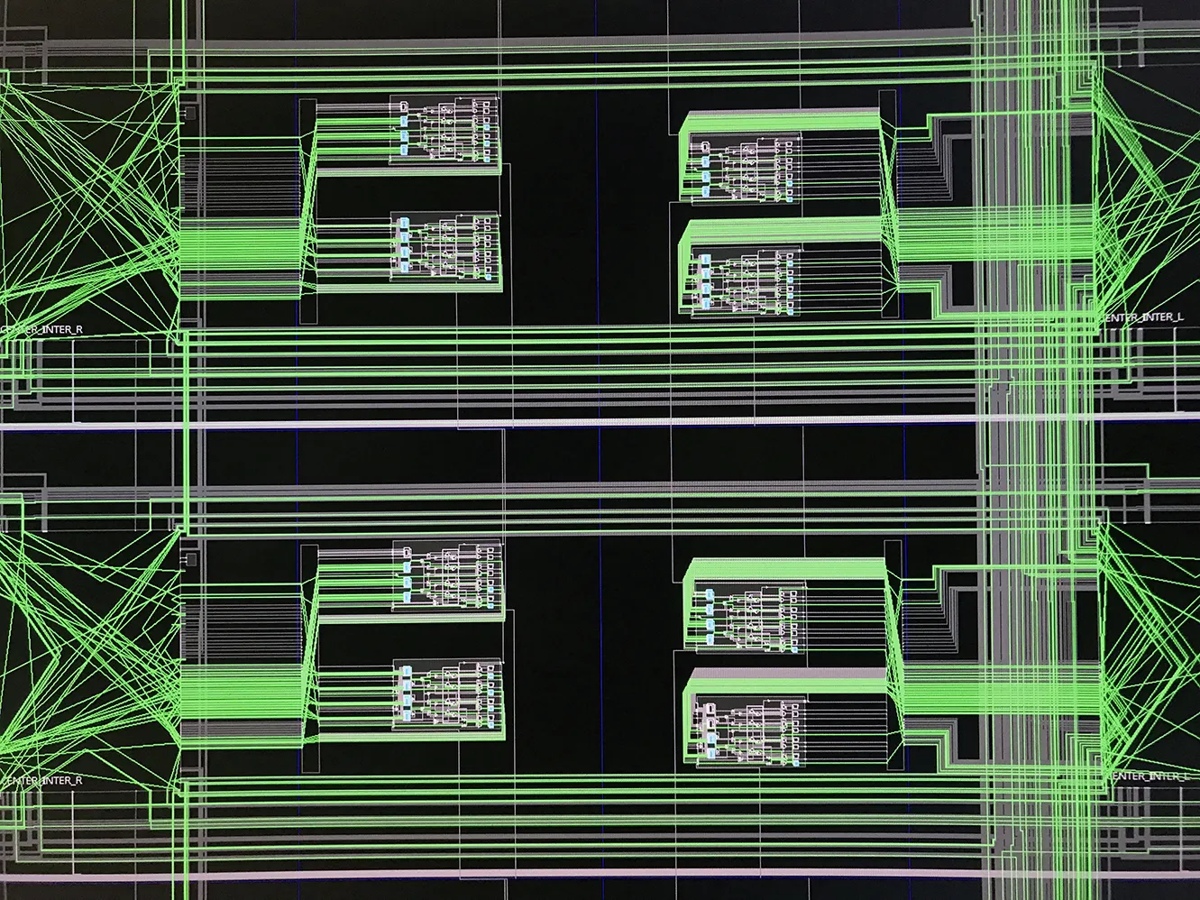
The GVPU executes a custom instruction set where one instruction is one 1024-bit word, streamed out of Artix DDR3 over AXI-Stream into an eight-deep burst FIFO. Every word carries an opcode, an operand, and the state of 200 test bus pins at once. Castor and Pollux run one GVPU each and drive half the bus apiece, which is where the 400 channels come from.
Instruction word
Opcodes
| Opcode | Value | Action |
|---|---|---|
| VEC | 0x01 | Execute one vector |
| VECLOOP | 0x02 | Execute, then repeat it operand times |
| VECCLK | 0x03 | Drive a clock pin through a low then high phase |
| NOP | 0xff | Burn a cycle |
Every pin slot is one of six codes in four bits, and stimulus and comparison live in the same word, so a single beat both drives the device and checks what came back. There is no separate compare pass.
Subvectors
| Subvec | Value | Meaning |
|---|---|---|
| 0 | 0000 | Drive low |
| 1 | 0001 | Drive high |
| X | 0010 | Don't care |
| H | 0011 | Expect high |
| L | 0100 | Expect low |
| C | 0101 | Clock |
A repeating vector holds its word in the pipeline and counts down the 216-bit operand locally, so a pattern that idles or clocks for thousands of cycles costs one fetch instead of thousands. Memory bandwidth stops limiting how long a test can run, and no starved cycle reaches the test bus as jitter.
On a mismatch the engine sets a bit in a 200-wide fail mask, one bit per pin, so a failure reports which pins mismatched rather than just that the test failed. A thirteen-state machine sequences it: memory burst, load and run, then test setup, run, fail reporting and cleanup.
A second mode tests the board's own memory. It writes a pattern into Artix DDR3, reads it back and CRCs it in flight: sixteen CRC64 engines run in parallel, one per 64-bit chunk of every 1024-bit beat, so a burst is checked at full width without slowing the stream. The computed CRC goes back to memory, and Linux compares it against a known value. The path runs from userspace through DMA, across the Zynq to the Artix, into DDR3.
End-to-end verification
The GVPU and DUT RTL run in Verilator behind a C++ shim that the unmodified kernel driver binds to. Driver ioctl and DMA calls resolve to direct AXI bus calls instead of silicon.
Regression then runs the whole path with no board on the bench: userspace application, through the library, through the driver, into the vector processing unit, out to the device under test.
The boards
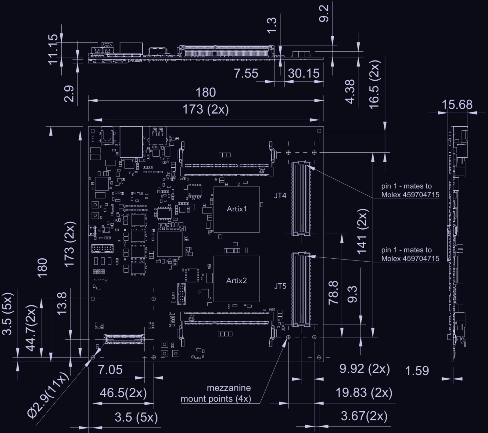
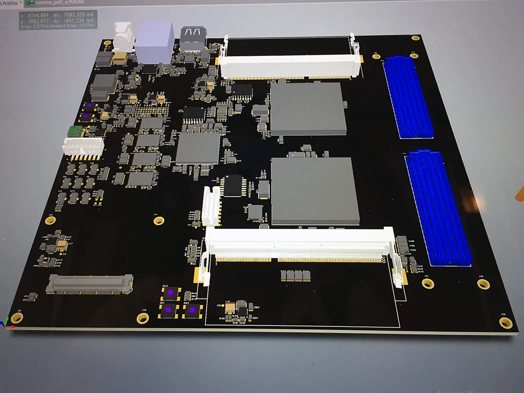
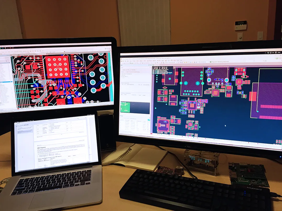
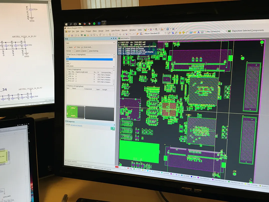
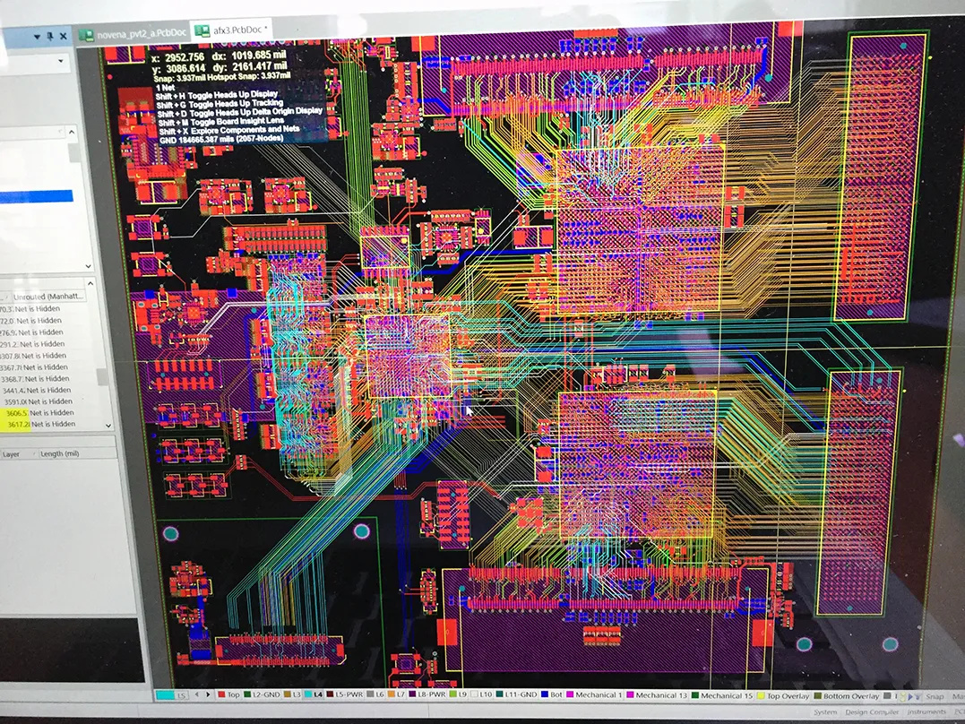
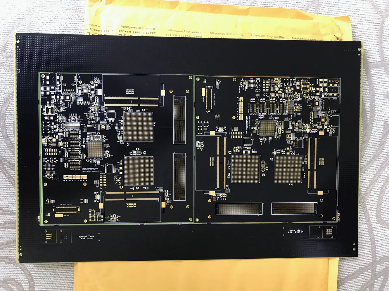
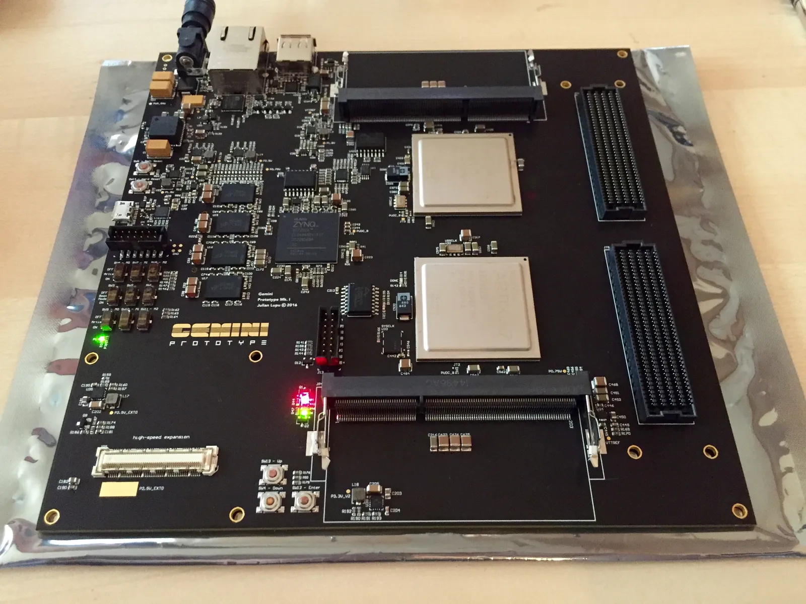
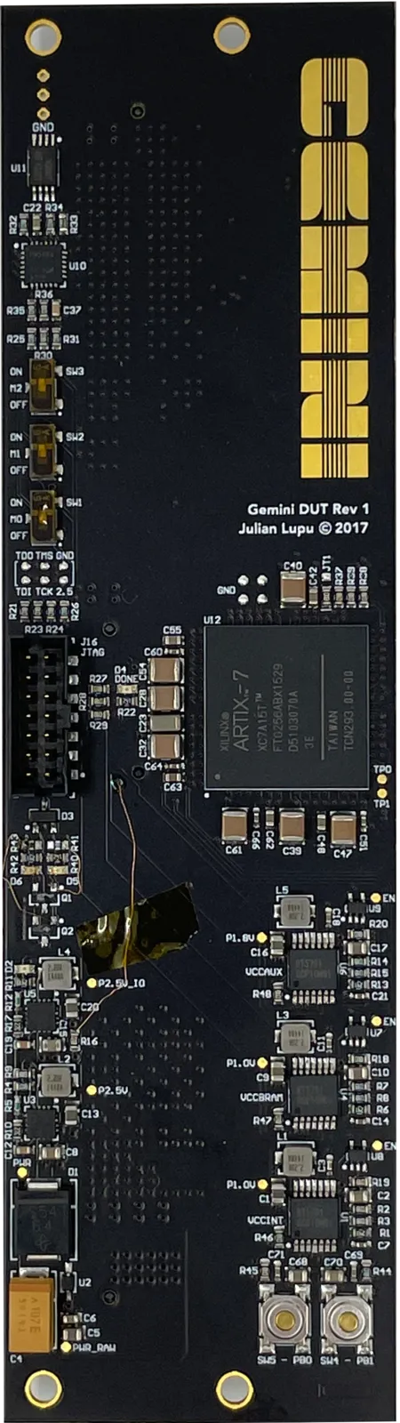
A 12-layer triple-FPGA motherboard and an 8-layer single-FPGA device-under-test validation board, both in Altium: board architecture, component selection, schematic capture and layout. Fine-pitch BGAs with high pin counts, DDR3 fly-by routing, impedance-controlled traces calculated against stack-ups from the board house. Power design and sequencing across three FPGAs, and interfaces to bring up for each: Gigabit Ethernet, USB 2.0, JTAG, UART, I2C, SD and SPI. Manufactured by Sierra Circuits.
Bring-up
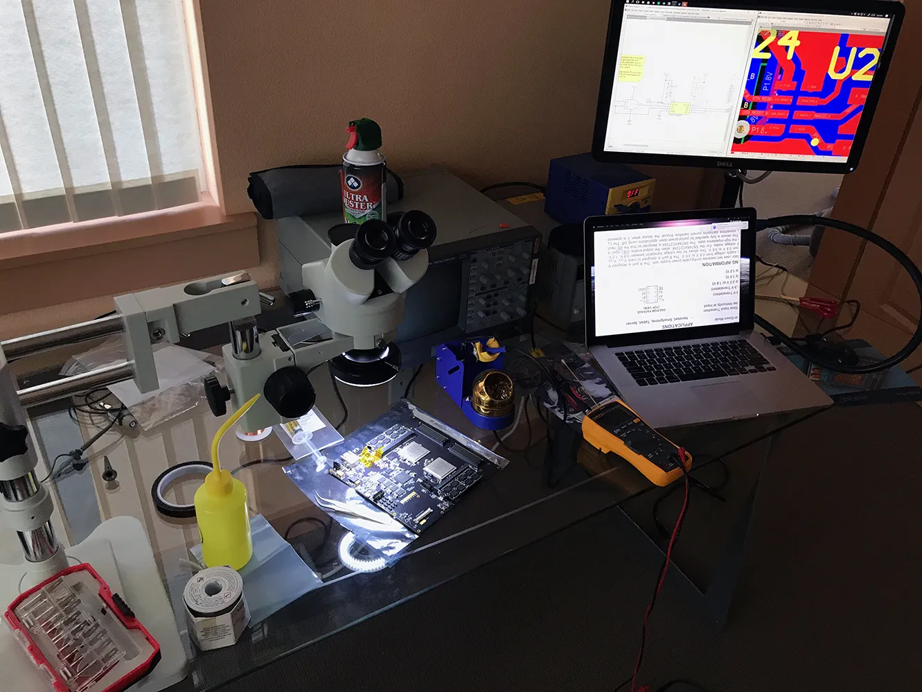
Debug and rework on a DMM, an oscilloscope, and a stereo microscope with a microsoldering iron.
Software
Test patterns are written in Dots. A Pins line names
the pins and fixes their order, and every vector after it is one
character per pin, in that order.
Pins RESET_B, IN, OUT

# release reset, then shift a one through
V0XX
V11L
V10H

# hold it for ten cycles
repeat 10 V10H
Those characters are the six subvector codes the hardware
executes, so a Dots file is close to a literal picture of what
lands on the test bus. repeat compiles to a
VECLOOP with its count in the operand, which is how
a thousand idle cycles cost one word of memory instead of a
thousand.
Leda compiles Dots into stim binaries. How those run is a separate file, a prgm, written in Fe, a small Lisp dialect with an API for loading patterns into tester memory and executing them.
(set-profile "board_profile.json")
(run
  (load "file1.stim")
  (load "file2.stim")
  (load "file3.stim"))
run stops at the first failing pattern and returns
how many ran, whether one failed, and the cycle it failed on.
runc runs everything regardless.
get-fail-pins returns which pins mismatched, which
is the 200-bit mask coming up from the engine.
Source code
Hardware documents
Mezzanine boards
Using it
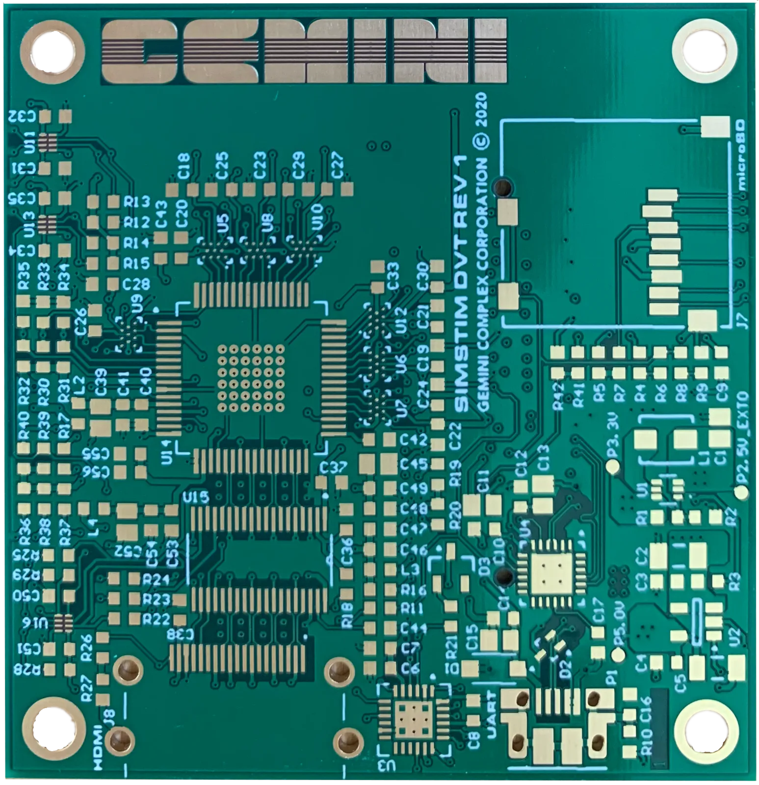
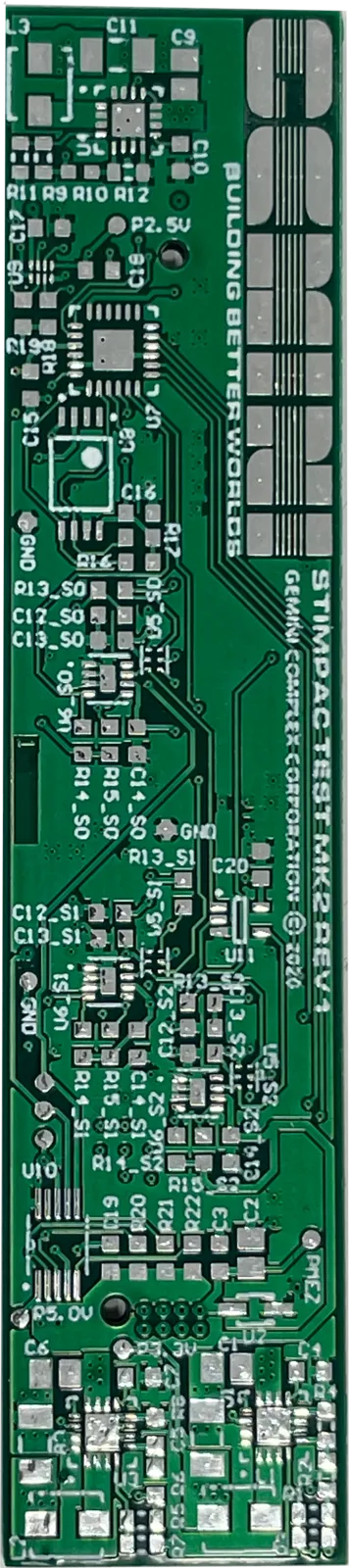
A DUT board mates to JT4 and JT5 and breaks the test bus out to whatever you are testing. You write Dots against the pins on that board, compile it with Leda, and queue a prgm from the web app. Agent runs it and returns pass or fail, the cycle it stopped on, and which pins mismatched.